

Appendix#
This appendix preserves an earlier Lacerta implementation approach for reference and educational purposes.
Early Lacerta Approach#
In this section, you can find the first approach considered for Lacerta:
a hierarchical hardening implementation strategy,
and a VGA-based approach for the display subsystem.
These alternatives were part of the early design exploration phase and helped define the final system direction.
Why This Approach Was Ruled Out#
Although the hierarchical hardening and VGA approach was technically valuable during development, it was eventually ruled out because of I/O pin limitations in the target integration environment.
The VGA-oriented implementation required more external interface resources than were practical within the available pad and integration constraints. Because of that, the project moved toward the current approach, which better fits the Caravel user-project wrapper limits.
Why It Is Kept in the Appendix#
This material is still kept in the appendix because it provides useful background on:
the early architectural decisions in Lacerta,
the tradeoffs involved in choosing a hardening strategy,
and the educational value of understanding a hierarchical hardening flow.
Even though this path was not selected for the final implementation, it remains a helpful reference for readers who want to study alternative integration strategies and learn from the project evolution.
Lacerta Layout#
The physical implementation of Lacerta has been actively exercised throughout the development process. Most RTL modules have already been synthesized, placed, and routed using the full RTL-to-GDSII flow, allowing early identification of integration, timing, and routing challenges.
The resulting layout views and design metrics are documented in the following subsection. These results have been instrumental in iterating key physical design aspects such as:
Floorplanning strategies
Buffer insertion and optimization
Clock and reset distribution
This iterative approach has significantly improved timing closure and overall design robustness.
To streamline integration and simplify timing closure, Lacerta adopts a mixed physical implementation strategy:
Flattened (hardened) blocks for smaller control and interface logic
Pre-verified macros for larger, timing-critical datapath modules
These modules will be merged into the top-level during physical implementation:
wb_slave_memory_mappedwb_slave_to_mem_sys_portscommand_arbiter_decoder
These modules will remain as standalone, pre-implemented blocks:
mask_generatorMemory subsystem (
mem_sys, buffers)Preserves validated register and pattern generators
VGA controller and UART
Reuse of validated timing and I/O logic
WB Slave to Memory Mapped#
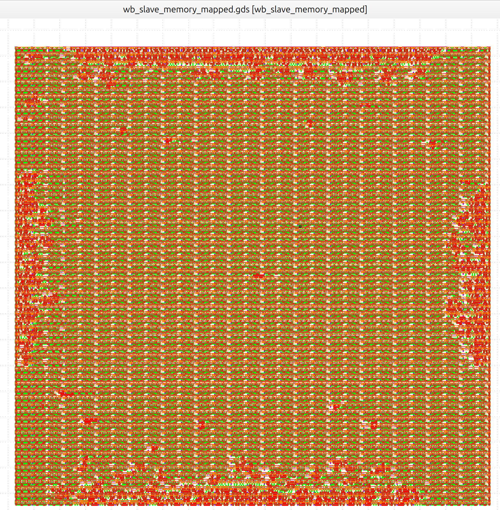
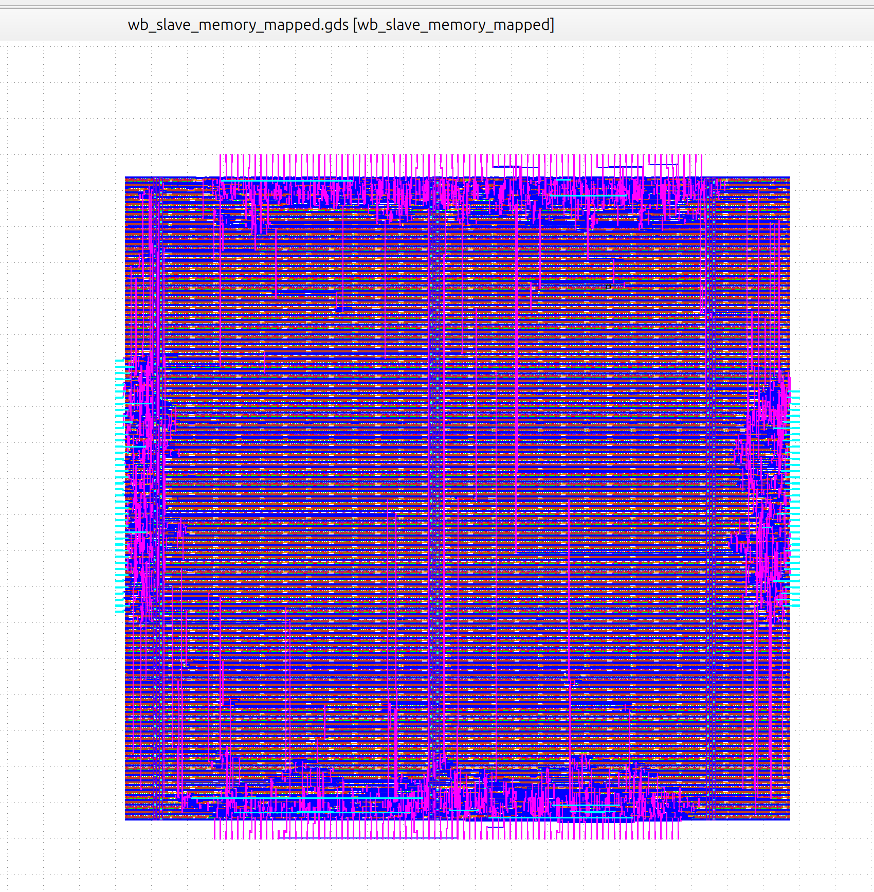
Layout of the Wishbone (WB) Slave to Memory-Mapped. The left image shows the cell placement without metal layers, highlighting the underlying standard-cell structure, while the right image includes the metal routing, illustrating the interconnections and signal wiring across the design.
Metric |
Value |
Notes |
|---|---|---|
Technology |
SKY130A |
Open PDK (config pdk::sky130*) |
Core Area |
0.131454 mm² |
design__core__area = 131454 µm² |
Die Area |
0.144400 mm² |
design__die__area = 144400 µm² |
Utilization |
10.86% |
design__instance__utilization = 0.108612 |
Standard Cell Count |
3,575 |
design__instance__count__stdcell |
Sequential Cell Count |
137 |
Sequential elements |
Routing Completion |
100% |
routing completed (no unrouted nets reported) |
Worst Negative Slack |
0.00 ns |
timing__setup__wns = 0.0 |
Total Negative Slack |
0.00 ns |
timing__setup__tns = 0.0 |
Max Frequency |
100 MHz (target) |
CLOCK_PERIOD = 10 ns |
Total Power |
1.531 mW |
reported power__total = 0.00153094 W |
DRC Violations |
0 |
no DRC errors reported |
LVS |
Passed |
layout vs netlist match reported |
Antenna Violations |
2 |
antenna__violating__nets = 2 |
GDS Generated |
Yes |
final |
WB Slave to Read/Write Ports#
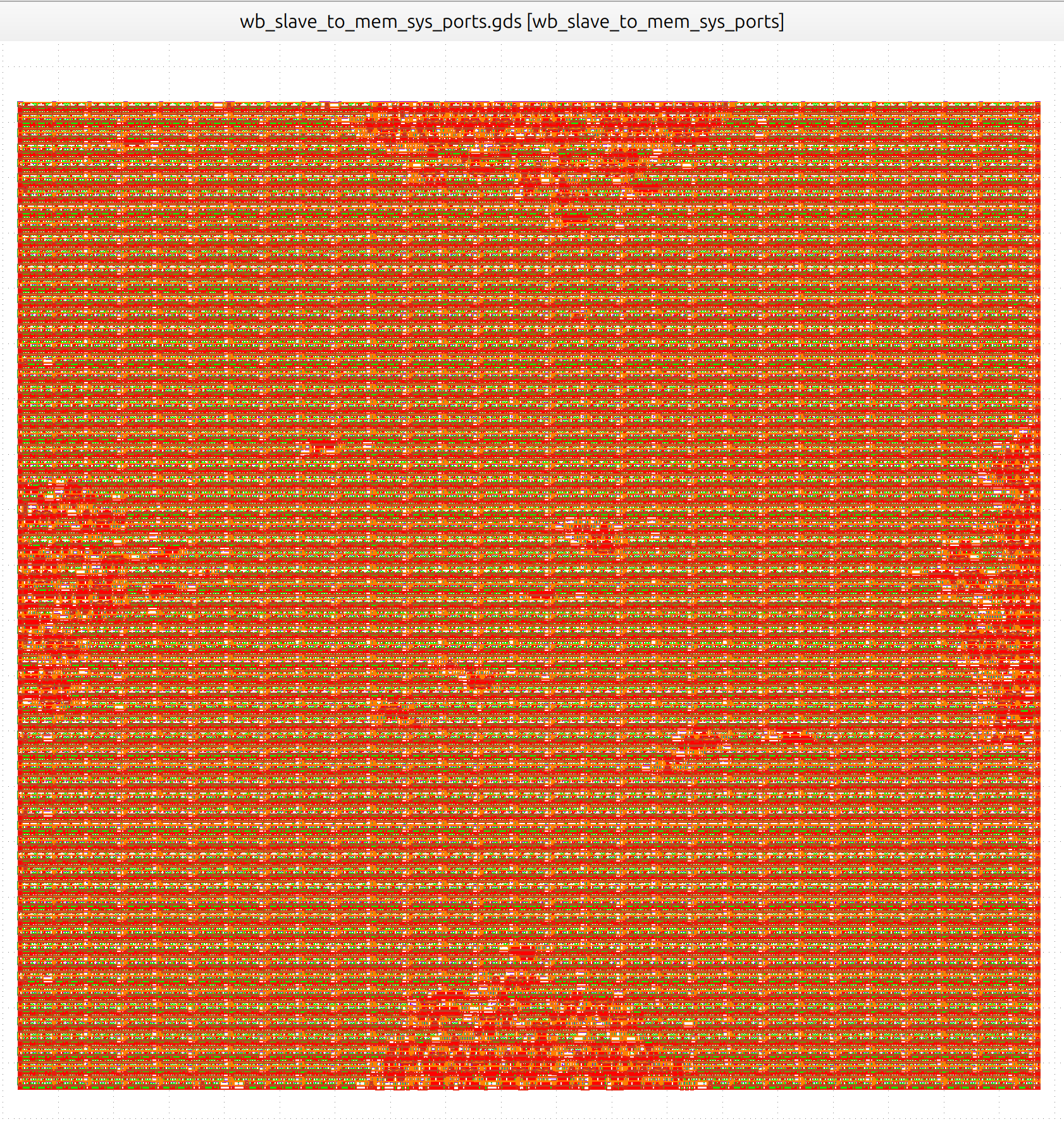
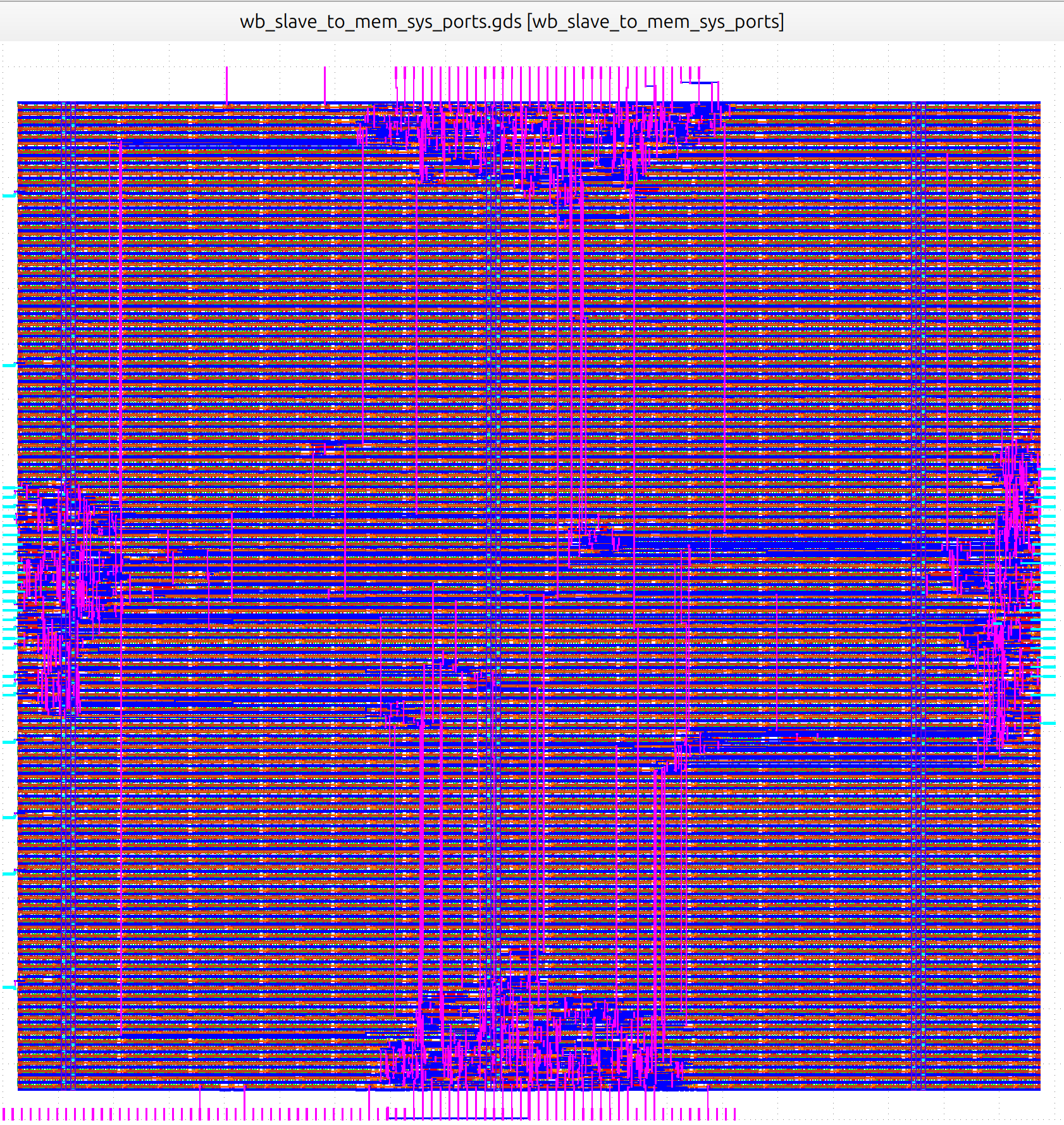
Layout of the Wishbone (WB) Slave to Read/Write Ports. The left image shows the cell placement without metal layers, highlighting the underlying standard-cell structure, while the right image includes the metal routing, illustrating the interconnections and signal wiring across the design.
Metric |
Value |
Notes |
|---|---|---|
Technology |
SKY130A |
Open PDK (config pdk::sky130*) |
Core Area |
0.131 mm² |
From 131,454 µm² |
Die Area |
0.144 mm² |
From 144,400 µm² |
Utilization |
7.19% |
Standard cell density |
Standard Cell Count |
2,898 |
Instance count |
Sequential Cell Count |
71 |
Sequential elements |
Routing Completion |
100% |
No unrouted nets |
Worst Negative Slack |
0.00 ns |
Timing met (no violations) |
Total Negative Slack |
0.00 ns |
No violations |
Max Frequency |
100 MHz (target) |
CLOCK_PERIOD = 10 ns |
Total Power |
0.934 mW |
Dynamic + leakage |
DRC Violations |
0 |
Magic + KLayout clean |
LVS |
Passed |
No errors reported |
Antenna Violations |
3 |
From routing report |
GDS Generated |
Yes |
Implied by completed flow |
VGA Controller#
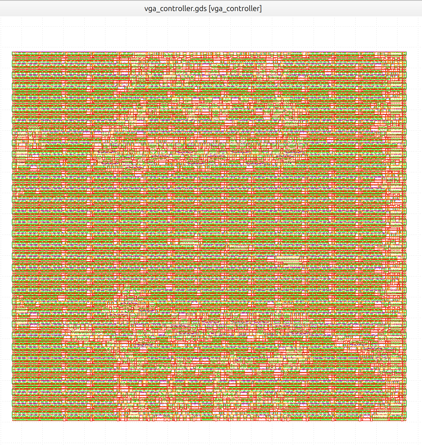
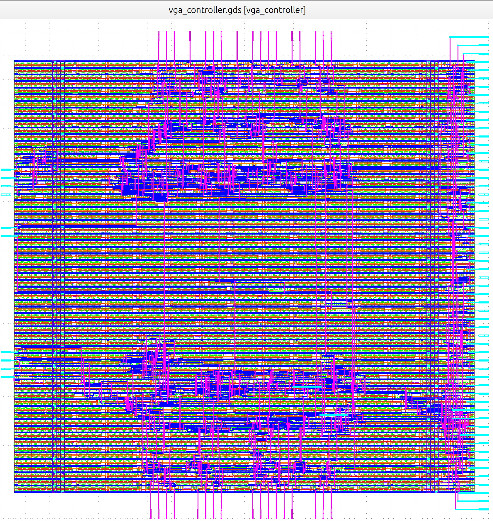
Layout of the VGA Controller. The left image shows the cell placement without metal layers, highlighting the underlying standard-cell structure, while the right image includes the metal routing, illustrating the interconnections and signal wiring across the design.
Metric |
Value |
Notes |
|---|---|---|
Technology |
SKY130A |
Open PDK (config pdk::sky130*) |
Core Area |
0.0333 mm² |
From 33,344.5 µm² |
Die Area |
0.0400 mm² |
From 40,000 µm² |
Utilization |
16.77% |
Standard cell utilization |
Standard Cell Count |
1,179 |
Std cell instances |
Sequential Cell Count |
24 |
Sequential elements |
Routing Completion |
100% |
No DRC routing errors |
Worst Negative Slack |
-0.95 ns |
Timing violation (worst case) at corner:max_ss_100C_1v60 |
Total Negative Slack |
-2.61 ns |
Setup violations present in corner:max_ss_100C_1v60 |
Max Frequency |
100 MHz |
Estimated from ~2.2 ns slack |
Total Power |
0.486 mW |
Dynamic + leakage |
DRC Violations |
0 |
Magic + KLayout clean |
LVS |
Passed |
No LVS errors |
Antenna Violations |
0 |
Clean |
GDS Generated |
Yes |
Flow completed successfully |
Command Arbiter Decoder#
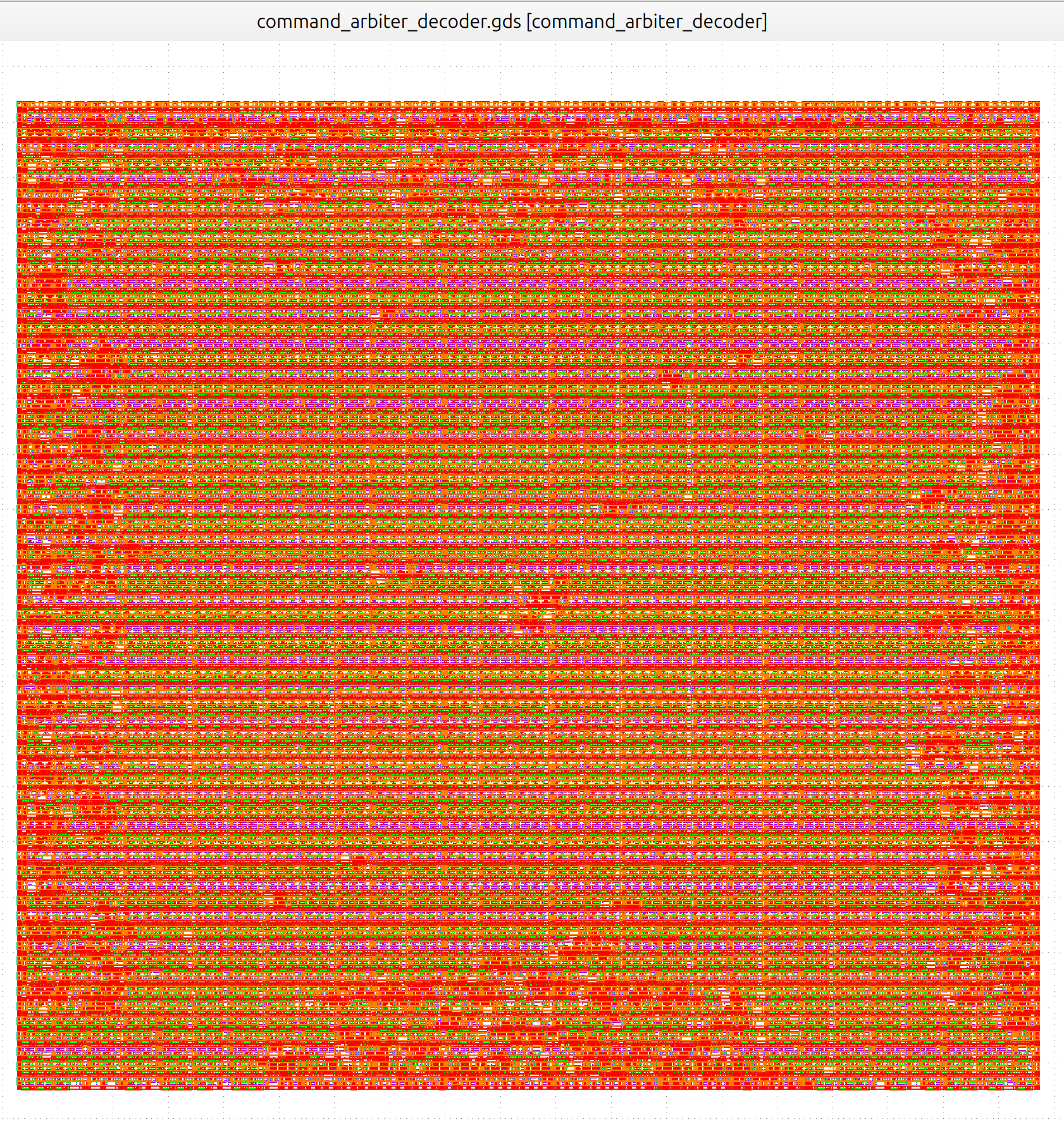
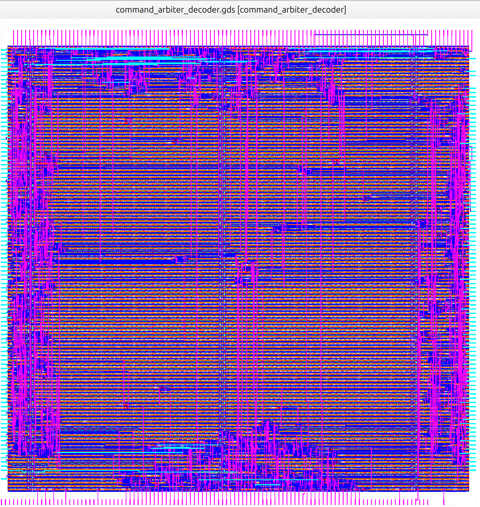
Layout of the Command Arbiter Decoder. The left image shows the cell placement without metal layers, highlighting the underlying standard-cell structure, while the right image includes the metal routing, illustrating the interconnections and signal wiring across the design.
Metric |
Value |
Notes |
|---|---|---|
Technology |
SKY130A |
Open PDK (config pdk::sky130*) |
Core Area |
0.1315 mm² |
From 131,454 µm² |
Die Area |
0.1444 mm² |
From 144,400 µm² |
Utilization |
7.19% |
Standard cell utilization |
Standard Cell Count |
2,898 |
Std cell instances |
Sequential Cell Count |
64 |
Sequential elements |
Routing Completion |
100% |
No unrouted nets |
Worst Negative Slack |
0.00 ns |
Timing met |
Total Negative Slack |
0.00 ns |
No violations |
Max Frequency |
~208 MHz |
Estimated from ~4.8 ns slack |
Total Power |
0.934 mW |
Dynamic + leakage |
DRC Violations |
0 |
Magic + KLayout clean |
LVS |
Passed |
No LVS errors |
Antenna Violations |
3 |
Minor violations present |
GDS Generated |
Yes |
Flow completed successfully |
Mask Generator#
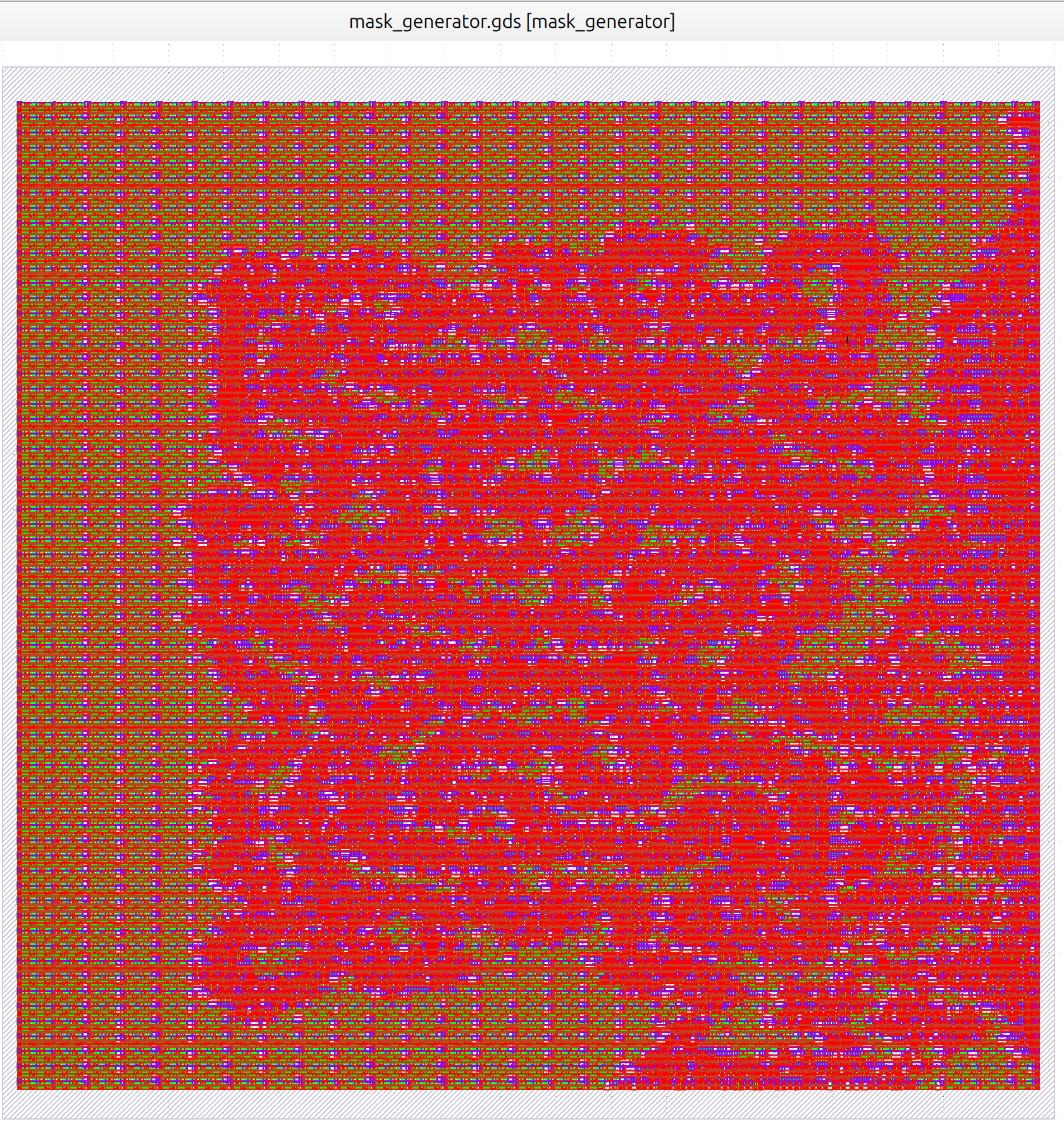
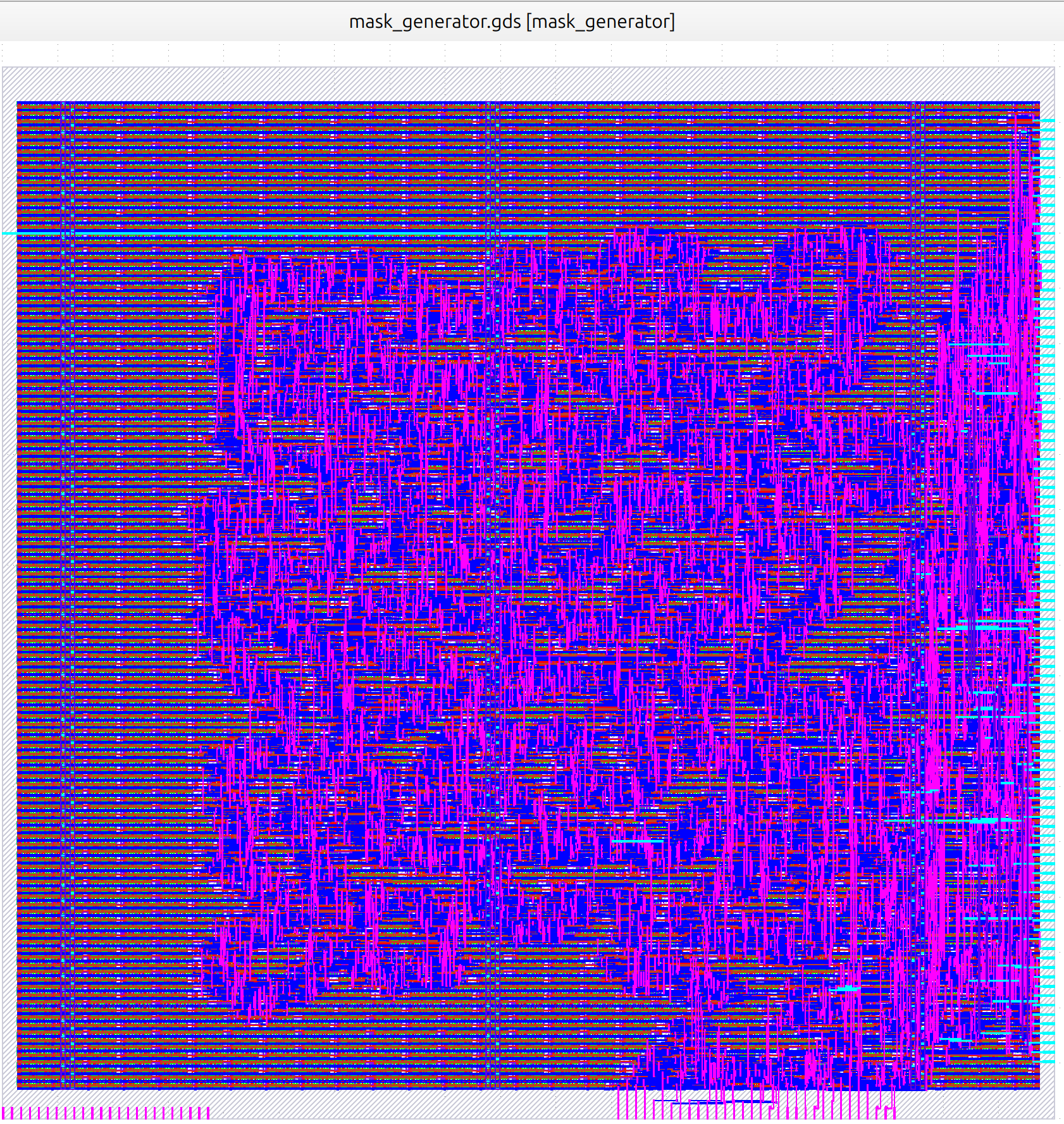
Layout of the Mask Generator. The left image shows the cell placement without metal layers, highlighting the underlying standard-cell structure, while the right image includes the metal routing, illustrating the interconnections and signal wiring across the design.
Metric |
Value |
Notes |
|---|---|---|
Technology |
SKY130A |
Open PDK (config pdk::sky130*) |
Core Area |
0.131 mm² |
From 131,454 µm² |
Die Area |
0.144 mm² |
From 144,400 µm² |
Utilization |
39.20% |
From 0.392 (stdcell utilization) |
Standard Cell Count |
7,471 |
Std cell instances |
Sequential Cell Count |
599 |
Sequential cells |
Routing Completion |
100% |
route__drc_errors = 0 |
Worst Negative Slack |
-0.36 ns |
timing__setup__wns |
Total Negative Slack |
-9.20 ns |
timing__setup__tns |
Max Frequency |
~100 MHz (target) |
CLOCK_PERIOD ≈ 10 ns (given) |
Total Power |
9.70 mW |
power__total (0.0097 W) |
DRC Violations |
0 |
Magic + KLayout clean |
LVS |
Passed |
No LVS errors |
Antenna Violations |
1 |
route__antenna_violation__count |
GDS Generated |
Yes |
Flow completed |
Memory System#
🚧 Content coming soon.
UART#
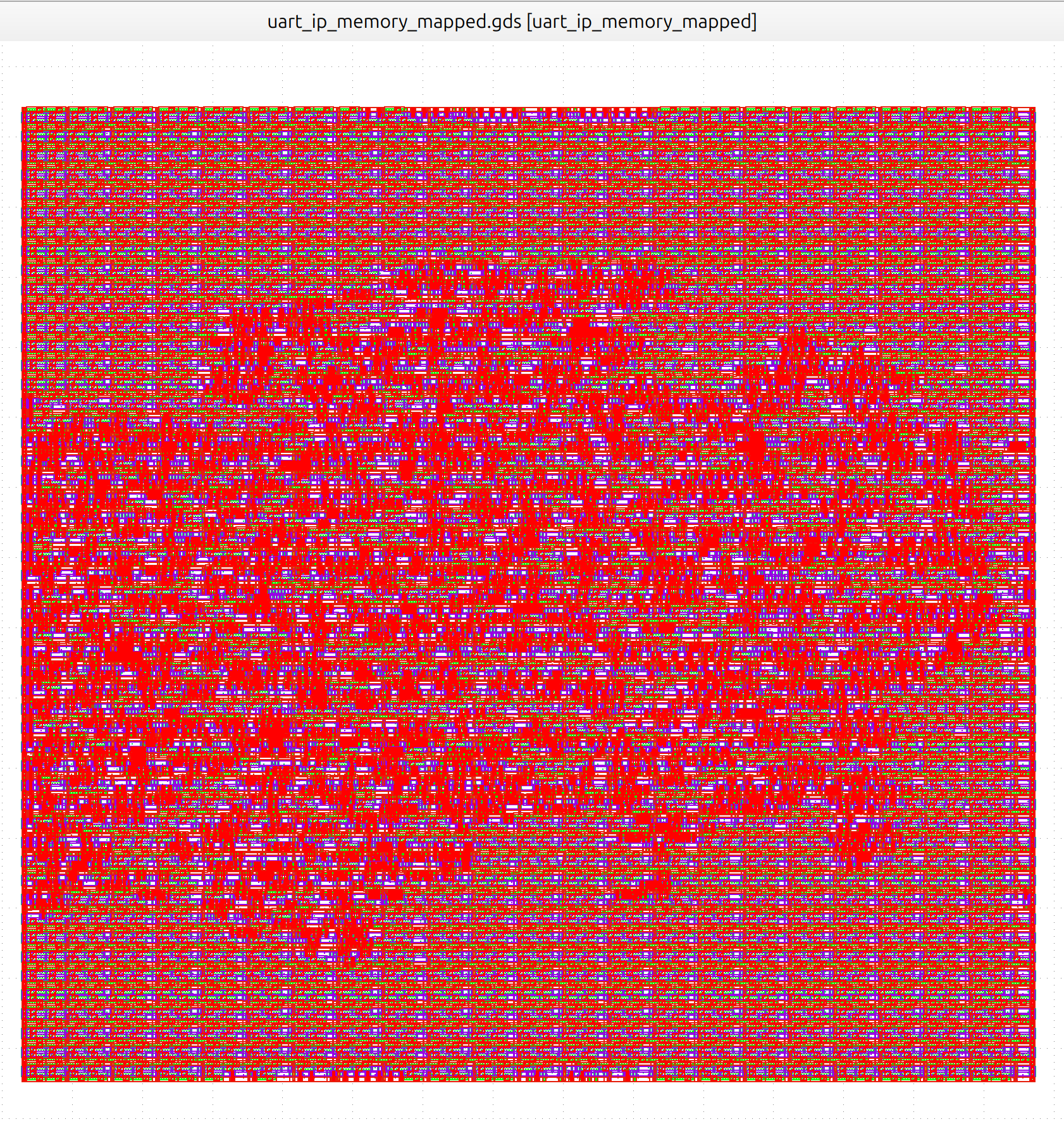
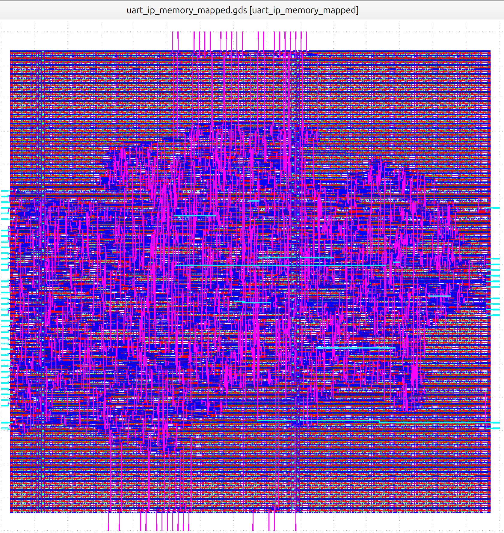
Layout of the UART. The left image shows the cell placement without metal layers, highlighting the underlying standard-cell structure, while the right image includes the metal routing, illustrating the interconnections and signal wiring across the design.
Metric |
Value |
Notes |
|---|---|---|
Technology |
SKY130A |
Open PDK (config pdk::sky130*) |
Core Area |
0.0801 mm² |
From 80,146.9 µm² |
Die Area |
0.0900 mm² |
From 90,000 µm² |
Utilization |
26.86% |
From 0.2686 (stdcell utilization) |
Standard Cell Count |
3,331 |
design__instance__count |
Sequential Cell Count |
278 |
design__instance__count__class:sequential |
Routing Completion |
100% |
route__drc_errors = 0 |
Worst Negative Slack |
0.00 ns |
timing__setup__wns |
Total Negative Slack |
0.00 ns |
timing__setup__tns |
Max Frequency |
~100 MHz (target) |
CLOCK_PERIOD ≈ 10 ns |
Total Power |
2.66 mW |
power__total (0.00266 W) |
DRC Violations |
0 |
Magic + KLayout clean |
LVS |
Passed |
No LVS errors (assumed from clean flow) |
Antenna Violations |
1 |
route__antenna_violation__count |
GDS Generated |
Yes |
Flow completed |